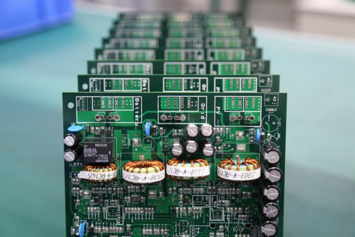
The practical realization of an electronic device is, simply put, the process by which all the components of that device are connected as a whole. This connection can be realized in many ways. Beginners use finished, very simple printed circuits consisting of narrow, parallel copper lines with drilled holes.
With a little skill, many electric circuits can be realized on them. However, the real solution that all electronics lovers come up with is printed circuit boards. Here we will briefly explain the process of making a printed circuit board as a DIY project.
Fabrication material
FR-2 and FR-4 are used to make PCBs, which can be single-sided and double-sided, ie. to have copper applied to one or both sides. The FR-2 is mainly used for prototypes and hobby purposes, while the high-quality tiles are used exclusively by the FR-4, although it can also be used for hobby purposes, but is slightly more expensive than the FR-2. The one-sided FR-2 will be very easy to spot by color ranging from light to dark brown and not transparent.
Although FR-4 is not transparent until the copper is removed, it is very easily distinguished from FR-2. The double-sided FR-2 is a little harder to distinguish at first glance than the FR-4 because both surfaces are covered with copper, so some experience is required. It is important that you know the difference and choose the right material according to your needs. Check this if you are not familiar enough with the concept of the PCB prototype.
Trimming
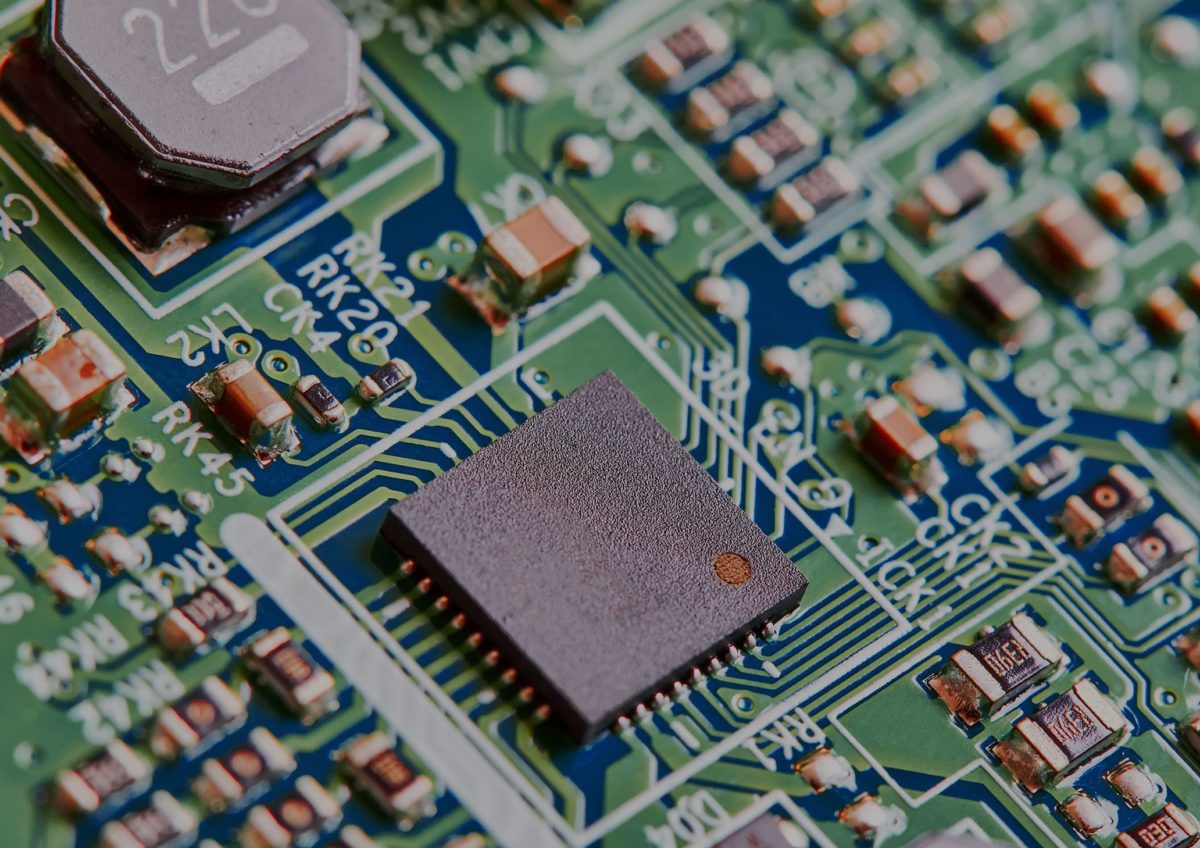
Since FR-2 is a very brittle material, care must be taken when cutting to prevent the plate from cracking where it is not needed. One of the safer ways is to use a scalpel; cut on both sides with a scalpel several times and simply break in a line. It is possible to cut it with something else, for example. scissors for sheet metal, but in this case, the edges are frayed and further processing is required.
We should also mention cutting with a small circular saw, but in this case it should be taken into account that the cut has a certain thickness, so care should be taken when marking the cutting line.
The FR-4 cannot be cut with a scalpel because it is very hard, but because of this it cuts the sheet metal shears well and can also be cut with a circular saw, but the low-quality saw will quickly become blunt due to its high hardness. If necessary, the edges should be trimmed with sandpaper or file after cutting.
Choice of paper
The first step is to select the paper to print the printed circuit board on the paper to be used. With all types of paper, it is not possible to achieve a proper transfer of laser toner from the same to the copper surface at the time when the paper is exposed to thermal heating by means of an iron.
For example, office A4 paper designed for everyday use may not give the same quality of laser toner transfer from paper to copper as glossy photo paper intended for professional photo printing.
Glossy photo paper gives great results, when you finish warming up the paper and then removing it, you can see that the laser is completely transferred to the copper surface, unlike standard print paper where laser toner cannot be transferred completely. You can try, but when you remove the paper from the copper, you will see that the quality is not very good and that some of the laser toner is still present on standard paper.
Copper surface cleaning
If the copper is oxidized or greasy due to finger contact, it should be cleaned in order to secure the protective material to the copper. Fine sanding or other abrasive material may be used to remove the oxidation, and degreasing is best used with dish detergent or similar.
Transferring laser toner to a surface
Transferring laser toner from glossy photo paper to the copper surface is done using an iron. The laser toner transfer process itself takes several tens of minutes, even up to half an hour. You have to do this part as best as you can and be patient, as the process itself comes down to ironing paper positioned on the copper surface of the tile. The more ironed the paper, the more confident the toner laser is to transfer to the copper surface. After 15 to 30 minutes, you can finish ironing, and then remove the paper from the copper surface.
Removing paper from the surface
After the ironing is complete, removal is followed. You have to be patient here, too, because if you pull abruptly, you may also have your laser toner removed, which will have to be done from scratch. If something like that happens, it can be frustrating because you have to start all over again.
It is removed by immersing it in lukewarm water and slowly removing it with gentle finger movements or using a toothpick, you can use both, but it is important to remove it slowly. After one part is removed, look into the same part, if there is no laser toner on the surface, this means that the thermal transfer has been done successfully and the toner remains on the surface. If all went well, you can be satisfied and continue to remove the rest.
This step can take up to an hour (depending on the size of the tile), but in the end when you remove it completely you can be happy with the results. That’s exactly what you wanted.
Corrosion of copper
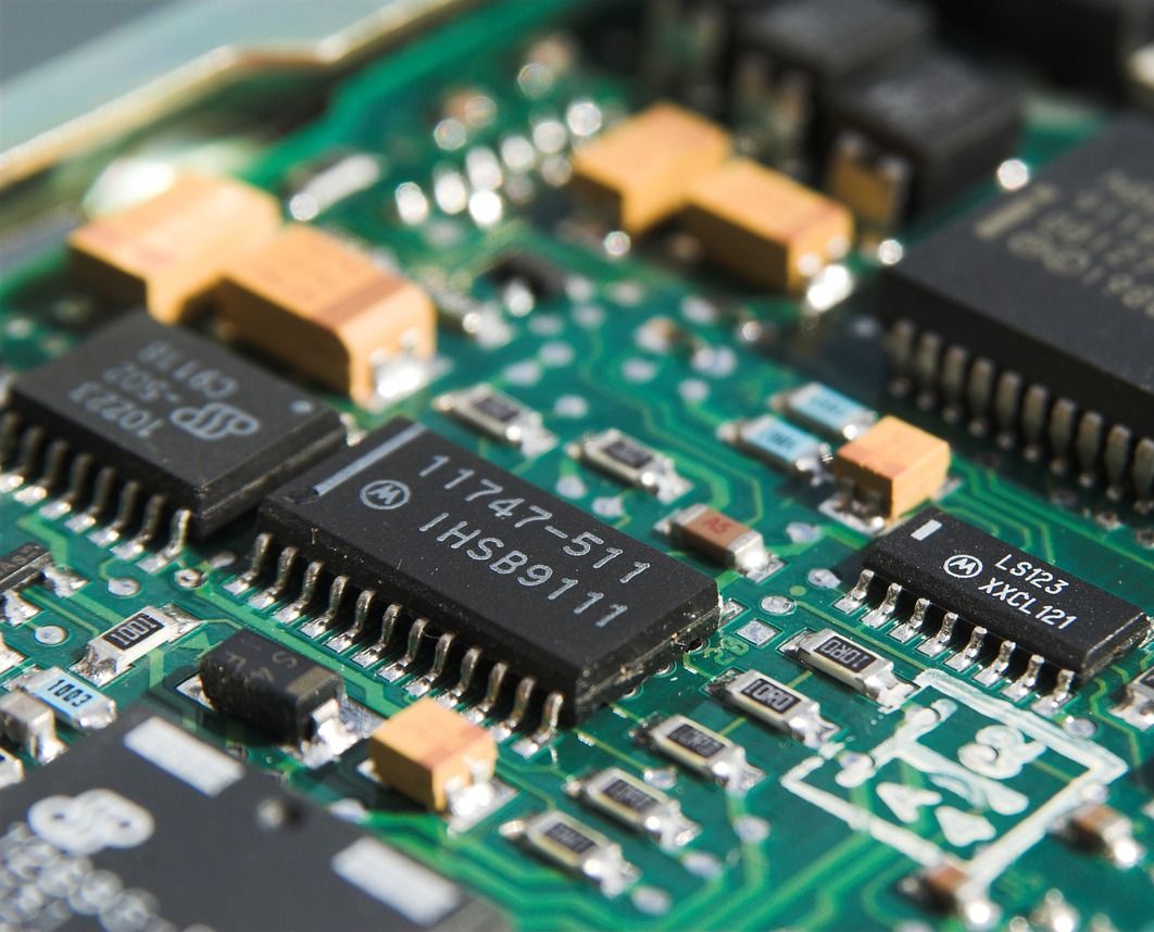
Corrosion is accomplished with a mixture of hydrochloric acid and hydrogen peroxide. Hydrochloric acid can be obtained at any store while hydrogen peroxide can be obtained from pharmacies. This is not the only way, you can do it with ferric chloride as well, it is your choice.
We opted for a mixture of hydrochloric acid and hydrogen peroxide by pouring hydrochloric acid into a plastic bowl or an old frying pan and then hydrogen peroxide in the amount sufficient to cause copper to erode. The mixture of hydrochloric acid and hydrogen peroxide has no effect on the laser toner.
This process is followed by washing the printed circuit board under lukewarm water and dishwashing detergent or laundry detergent. Protect your face and hands during corrosion as the mixture can irritate the skin if it comes in contact with it.
After washing the printed circuit board, the process of making it is completed and you will be very pleased. The next step is drilling holes, assembling electromechanical components and testing the device. If all tests pass, including all measurements, you can be satisfied, your prototype works!
Conclusion
As you can see, making printed circuit boards is not a particularly complicated job. However, for the first time, it might be advisable to practice with a piece of FR-2 first, and only then to create tiles that you will later use to make a device.


